CXMT packaging: 40 / 30 / 20, and the plant that takes the stack in-house
Packaging is two businesses wearing one name, and the split between them decides who keeps the value when the memory cycle turns.
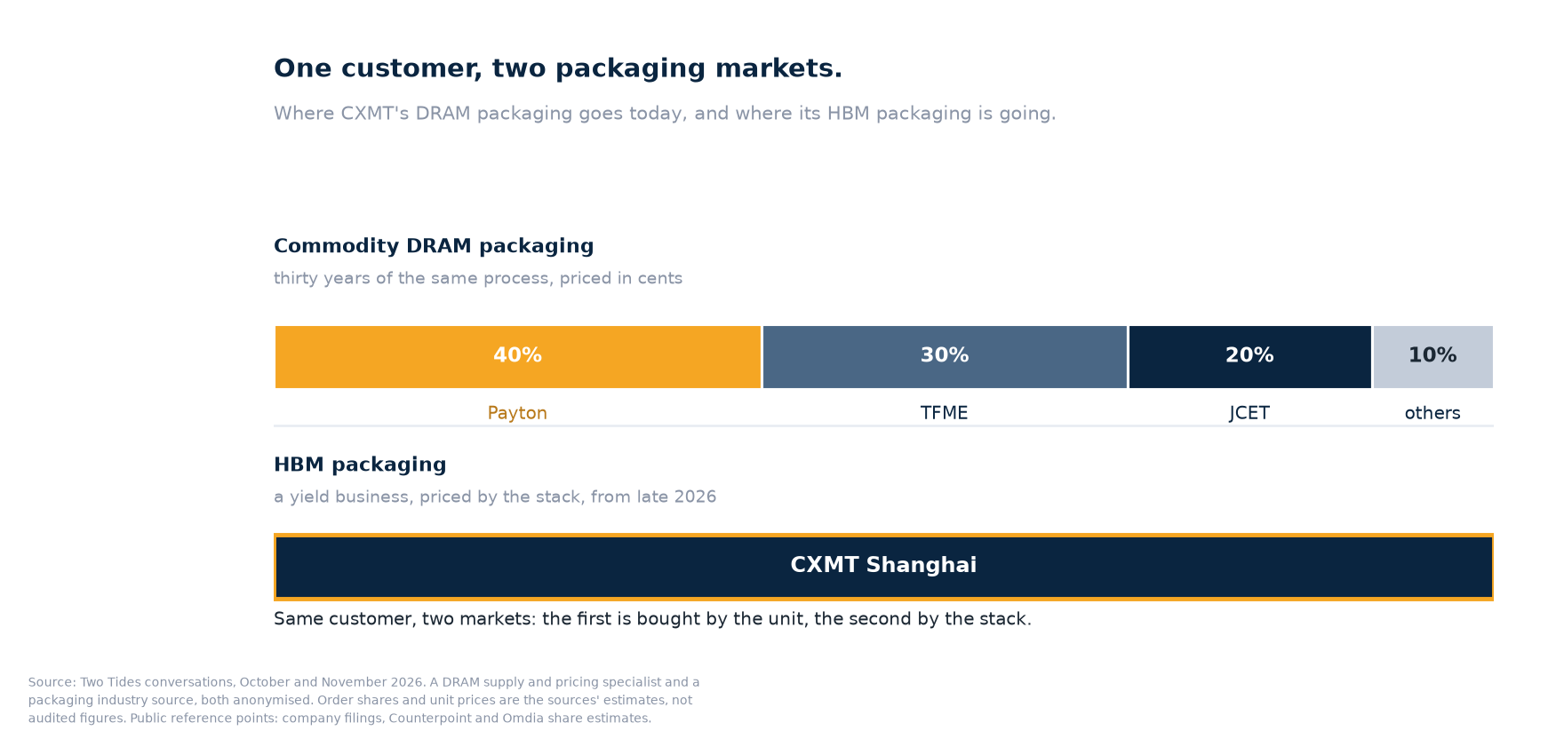
- 40 / 30 / 20the split of CXMT's DRAM packaging orders across Payton, TFME and JCET, on the source's estimates
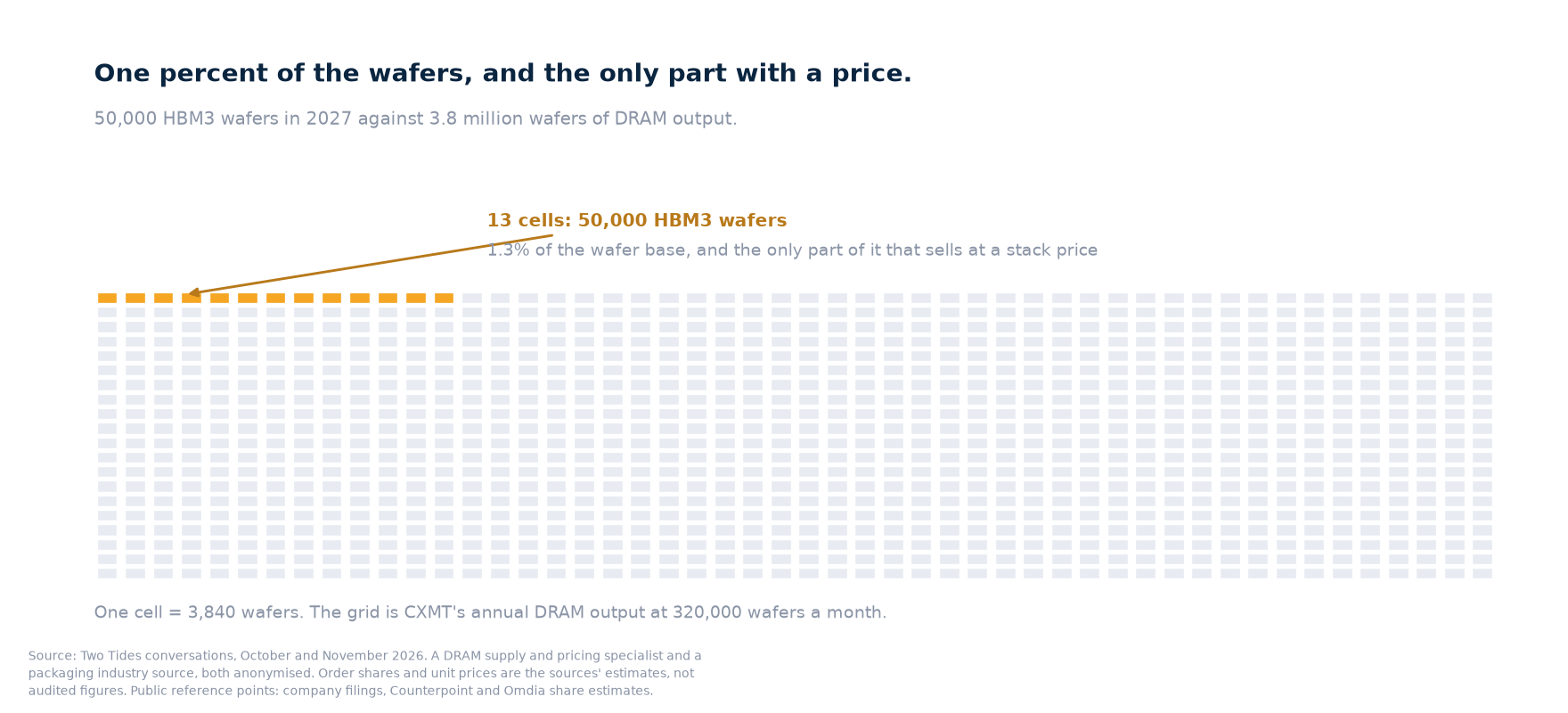
- 1.3%the share of CXMT's wafer base that goes to HBM3 in 2027: about 50,000 wafers against 3.8 million of output
- 25%CXMT's reported HBM3 yield, with the loss concentrated in stacking rather than the base DRAM
CXMT listed in Shanghai in July 2026, closed the first session up 466%, and ended the quarter with somewhere between 7% and 10% of global DRAM revenue depending on the tracker. It runs about 320,000 wafers a month, aims for 350,000 by the end of the year, and outsources its DRAM packaging to three houses: Payton in Hefei, TFME and JCET. At the same time it is building an HBM packaging plant in Shanghai, due to start production around the end of 2026, on the site where the HBM wafers themselves are made. Packaging is two businesses wearing one name, and the split between them decides who keeps the value.
Who does what today
| House | Order share | Products | Revenue from CXMT, 2025 |
|---|---|---|---|
| Payton (Shenzhen Kaifa) | ~40% | WBGA wire bond, FCCSP; DDR2–DDR4, LPDDR3/4 | ~2.4B yuan |
| TFME | ~30% | stacking and bumping; LPDDR5, GDDR5/6 | ~0.8B yuan; ~1.8B guided for 2026 |
| JCET | ~20% | stacking and bumping; LPDDR5, GDDR6 | not disclosed |
The volume position earns more than the value position: Payton ships the oldest packages at prices counted in cents and still books three times TFME's revenue from the same customer. Traditional storage packaging remains a wire-bond business with margins near zero, and only CXMT among memory makers has moved its own products onto advanced packaging flows.
Why the stack goes inside the fab
The HBM3 guided for 2027 is about 50,000 wafers, a little over 1% of a 3.8 million wafer year, against a public capacity nameplate of 60,000 wafers a month that the shipment figure cannot be read against without knowing the unit. Reported yield is near 25%, with most of the loss in stacking. The incumbents keep the stack in-house at every generation: moulded underfill at SK Hynix, hybrid bonding confined to the base die at Samsung, thermal compression with a non-conductive film at Micron, and full hybrid bonding at twenty layers for HBM5, which requires chemical mechanical polishing and an ISO class 3 cleanroom, both wafer-fab disciplines that assembly houses do not run.
What would change the picture
Watch TFME's revenue from this customer after the Shanghai plant ramps: if it keeps climbing past 1.8 billion yuan into 2028, the plant is a fab-side addition and the houses keep the assembly; if it flattens while HBM volume grows, the stack has been substituted in-house. Watch the plant's first full quarter of output in the first half of 2027. And watch the HBM3 shipment number against the 60,000 nameplate, because the ratio between them is the utilisation of a plant that has not yet been described in units that reconcile.
The analysis behind these numbers runs nine sections: the two packaging markets behind one name, who earns what from the same customer, and the counter-argument from the houses themselves.
Read it in Two TidesThis page is the public data companion to Tide 009 in Two Tides. The complete argument, with both sources' figures reconciled in the text, is the post in the letter.
Research, not advice. This page is research and commentary on an industry. It is not investment, legal or engineering advice, and not a recommendation to buy or sell any security. Figures are the best estimate available at the time of writing; where one rests on a single source, the text says so.
Cite this page as: Quorsio, "CXMT packaging: 40 / 30 / 20, and the plant that takes the stack in-house", November 2026, with a link to this URL. Short excerpts with attribution are welcome. Republishing the page in full, including its tables and charts, needs written permission: hello@quorsio.com.