Domestic AI packaging: 210,000 wafers a year, twice what the 2027 forecast needs
The arithmetic anyone can redo: capacity times good dies per wafer, against a forecast of 2.8–3.0 million chips. What is scarce is the seam, not the line.
- 210k–220kwafers a year of domestic CoWoS-S and CoWoS-L capacity by the end of 2026, the source's estimate
- 5–7Mgood dies those lines release once 25 to 40 good dies per wafer are applied
- 2.8–3.0Mthe 2027 Ascend forecast they have to serve, and the number the whole argument is about
Every public argument about Chinese AI chips arrives at the same worry: once the fabs lift yield, the bottleneck moves into advanced packaging and the assembly houses become the ceiling. The arithmetic does not support it. Domestic packaging is not the scarce input in 2027, and the shortage that does exist sits in a handoff no company in the country runs end to end.
Who holds the lines
On the S format, the workhorse behind nearly every AI chip shipping today, three houses hold the first tier, and both TFME and JCET's advanced packaging arm are climbing toward 3,000 wafers a month by year-end. A second tier is commissioning now at roughly 1,000. On the L format, the larger package that prints wiring on the substrate instead of an interposer, only three houses hold meaningful capacity, and TFME is not one of them yet.
| House | CoWoS-S now | CoWoS-S by year-end | CoWoS-L now | S / L load |
|---|---|---|---|---|
| SJ Semiconductor | 6,000–7,000/mo | roughly steady | ~30,000/yr | 90% / 70% |
| JCET (advanced packaging arm) | ~2,000/mo | ~3,000/mo | ~10,000/yr | ~80% / ~80% |
| TFME | ~2,000/mo | ~3,000/mo | building to 2027 | ~80% / n.a. |
| Ningbo-based entrant | n.a. | n.a. | ~5,000/yr | n.a. / ~50% |
The multiplication nobody publishes
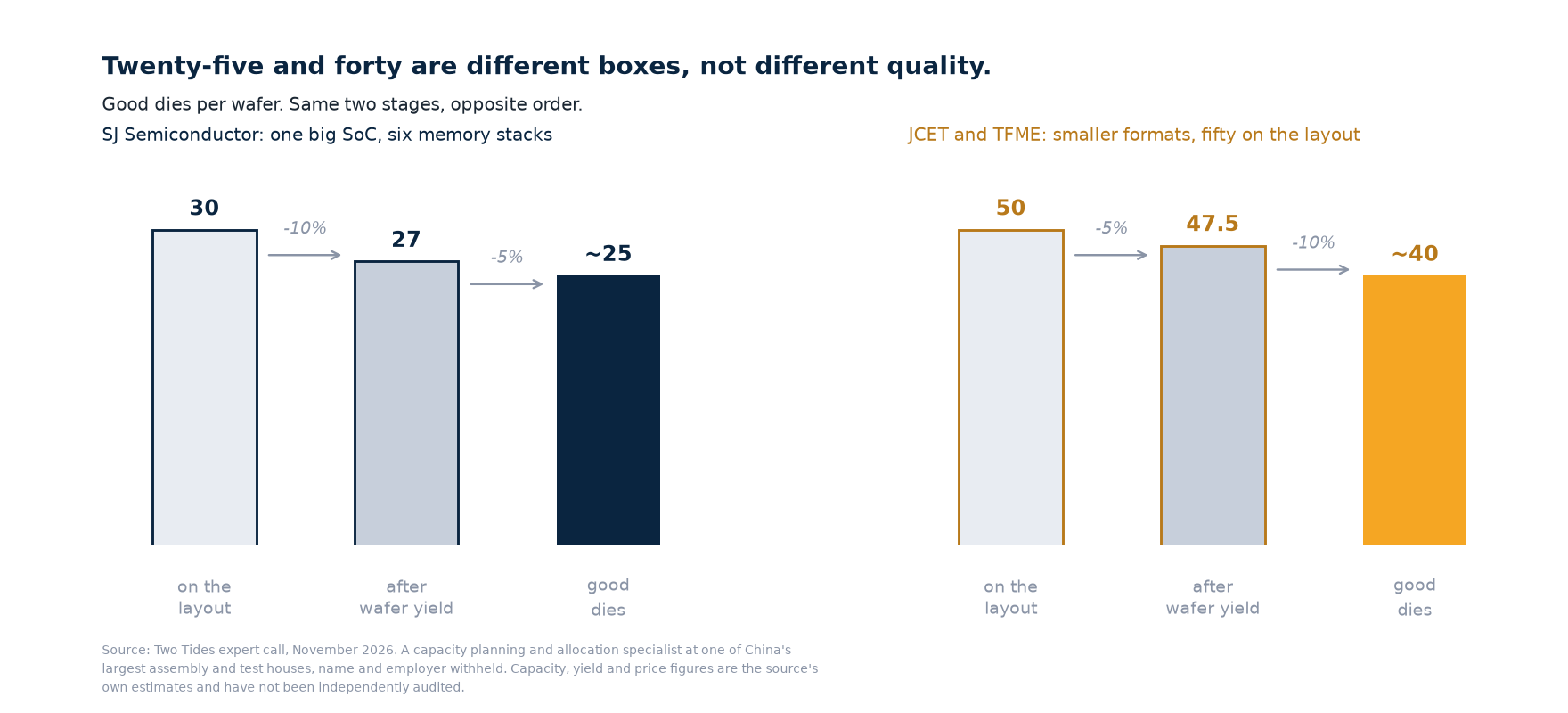
Every wafer yields a known number of good dies, measured on running lines rather than projected. SJ cuts 30 dies per wafer on its flagship, runs wafer yield above 90 percent and packaging yield around 95, and lands near 25. JCET and TFME cut about 50, run the same stages in the opposite order, and land near 40. Apply the conservative count across the 210,000 to 220,000 wafer base and the lines release about five million good dies; blended toward the larger counts, six or seven million.
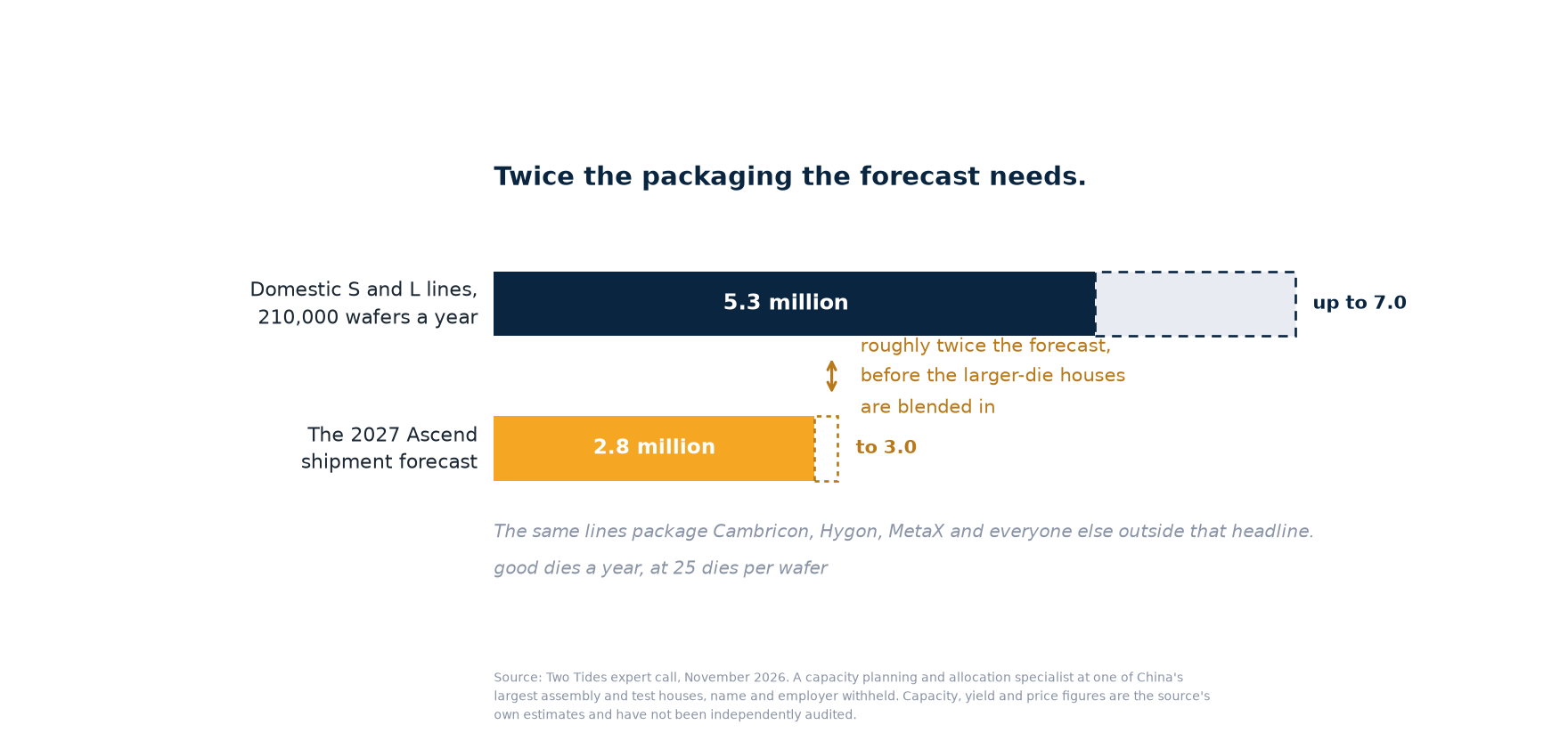
Against that, the entire 2027 Ascend forecast is 2.8 to 3.0 million chips, and these houses also serve Cambricon, Hygon and MetaX outside that headline. Even the conservative count carries roughly double the load. Two caveats: mix matters, and capacity is not capability.
Why twenty-five is not a quality problem
The gap between 25 good dies and 40 reads like quality and is not. SJ runs one large SoC with six memory stacks, a package big enough that only 30 fit on a wafer before yield takes its share. JCET and TFME run smaller formats that cut 50, and their yield structure inverts: better at the wafer stage, weaker at assembly. They build different boxes, and a single packaging yield figure flatters whoever runs the smaller die. See die yield for why the stages multiply either way.
The seam
Every tier-one house can stack memory, and every tier-one house can run 2.5D integration, but none does both as one flow under one roof: the memory work that exists serves domestic designers through trials, and none of it enters an AI chip. The full HBM-to-2.5D sequence still depends on supply from outside the country. The constraint moved into the seam between two buildings with different yield accountability, which the TSMC capacity picture makes legible.
What would shrink the headroom
Three things are checkable without a source: the year-end run rate against 210,000 to 220,000 wafers, TFME's L line guided to 1,000 wafers a month by the end of 2027, and whether any house announces a closed memory-stack plus 2.5D flow. That announcement, more than any capacity number, is the moment the bottleneck picks a home. Until then the restraint holds and prices stay polite until about 2028, when the 2027 forecast gets its answer.
The issue works the full ladder: the customer map that was fixed years before AI packaging existed, the L format's upstream lock, what a second-tier entrant actually faces when it courts a customer, and the 2028 date everyone is quietly working toward.
Read it in Two TidesThis page is the public data companion to Two Tides Issue 008. The complete argument, including the customer map and the entry economics, is the issue in the letter.
Research, not advice. This page is research and commentary on an industry. It is not investment, legal or engineering advice, and not a recommendation to buy or sell any security. Figures are the best estimate available at the time of writing; where one rests on a single source, the text says so.
Cite this page as: Quorsio, "Domestic AI packaging: 210,000 wafers a year, twice what the 2027 forecast needs", November 2026, with a link to this URL. Short excerpts with attribution are welcome. Republishing the page in full, including its tables and charts, needs written permission: hello@quorsio.com.